Description
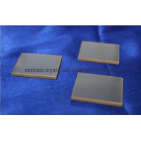
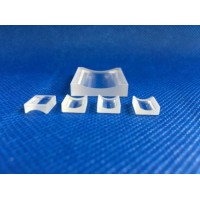
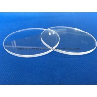
Product Name: Ge Mono Wafer Ge Window Germanium Windows Ge Lens/Optical Lens Model NO.: D1"~D8" Coating: Polish Customized: Customized Certification: RoHS, ISO9001 Lenses Color: Grey Material: Ge Mono Shape: Round Transmittance: >95% Type: Flat Lens Usage: Optical HS Code: 9001909090 Product Description Single crystal (Ge)Germanium WaferGe wafer:Germanium (Ge) is the preferred lens and window material for high performance infrared imaging systems in the 8-12 um wavelength band. Its high refractive index makes Ge ideal for low power imaging systems because of minimum surface curvature. Chromatic aberration is small, often eliminating the need for correction.Germanium is most widely used for lenses and windows in IR systems operating in the 2 um - 12 um range. Its transmission is very temperature sensitive, becoming opaque near 100°C. Environment does not cause problems because Germanium is inert, mechanically rugged, and fairly hard.Germanium is a high index material that is used to manufacture Attenuated Total reflection (ATR) prisms for spectroscopy. Its refractive index is such that germanium makes an effective natural 50% beamsplitter without the need for coatings. It is also used extensively as a substrate for production of optical filters. Germanium covers the whole of the 8-14 micron thermal band and is used in lens systems for thermal imaging. It can be AR coated with diamond producing an extremely tough front optic.Application as window, lens, beamsplitter, ATR prism or filter in spectrometers and in thermal imaging.Specifications:Ge wafer:Material:GeDimension Tolerance+0.0, -0.1mmThickness Tolerance:± 0.1mmSurface quality:60/40Clear Aperture:>85%Flatness:λper 25mmParallelism:3'Bevel:<0.25mm X 45°Coating:Upon requirementGeneral Properties of Germanium WaferGeneral PropertiesStructureCubic, a = 5.6754 ÅDensity:5.765 g/cm3Melting Point:937.4 oCThermal Conductivity:640Crystal Growth TechnologyCzochralskiDoping availableUndopedSb DopingDoping In or GaConductive Type/ NPResistivity,ohm.cm>35 <0.05 0.05 - 0.1EPD< 5x10³/cm2< 5x10³/cm2 < 5x10³/cm2 < 5x10²/cm2< 5x10²/cm2< 5x10²/cm2 Grades and Application of Germanium waferElectronic GradeUsed for diodes and transistors,Infrared or opitical GradeUsed for IR optical window or disks,opitical componentsCell GradeUsed forsubstrates of solar cellStandard Specs of Germanium Crystal and waferCrystal Orientation<111>,<100> and <110> ± 0.5oor custom orientationCrystal boule as grown1" ~ 6" diameter x 200 mm LengthStandard blank as cut1"x 0.5mm2"x0.6mm4"x0.7mm5"&6"x0.8mmStandard Polished wafer(One/two sides polished)1"x 0.30 mm2"x0.5mm4"x0.5mm5"&6"x0.6mmSpecial size and orientation are available upon requested Wafers4 inch Ge wafer SpecificationDopingPDoping substancesGe-GaDiameter100±0.25 mmOrientation(100) 9° off toward <111>+/-0.5Off-orientation tilt angleN/APrimary Flat OrientationN/APrimary Flat Length32±1mmSecondary Flat OrientationN/ASecondary Flat LengthN/Ammcc(0.26-2.24)E18/c.cResistivity(0.74-2.81)E-2ohm.cmElectron Mobility382-865cm2/v.s.EPD<300/cm2Laser MarkN/AThickness175±10μmTTV<15μmTIRN/AμmBOW<10μmWarp<10μmFront facePolishedBack faceGroundGermanium Wafer ProcessIn thegermanium waferproduction process, germanium dioxide from the residue processing is further purified in chlorination and hydrolysis steps.1)High purity germanium is obtained during zone refining.2)A germanium crystal is produced via the Czochralski process.3)The germanium wafer is manufactured via several cutting, grinding, and etching steps.4)The wafers are cleaned and inspection. During this process, the wafers are single side polished or double side polished according to custom requirement,epi-ready wafercomes.5)The wafers are packed in single wafer containers, under a nitrogen atmosphere.Application:Germanium blank or window are used in night vision and thermographic imaging solutions for commercial security, fire fighting and industrial monitoring equipment. Also, they are used as filters for analytical and measuring equipment, windows for remote temperature measurement, and mirrors for lasers.Thin Germanium substrates are used in III-V triple-junction solar cells and for power Concentrated PV (CPV) systems.