详细说明
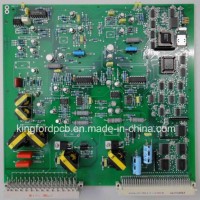
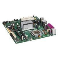
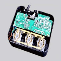
Product Name: OEM/ODM Shenzhen Printed Circuit Board PCBA Board Brand: ODM/OEM Insulation Materials: Epoxy Resin base Material: Copper Processing Technology: Electrolytic Foil Flame Retardant Properties: V0 Application: Consumer Electronics Material: Paper Phenolic Copper Foil Substrate Dielectric: FR-4 Type: Combining Rigid Circuit Board Certification: Pohs,CCC,ISO,Ts16949 Mode of Product: SMT+DIP Layers: Multilayer Max Size: Lenght:1500mm Width:520mm PCB Layer: 1-30 Board Size: 1500*600m Solder Mask Colour: Green,Blue,Yellow,Red,Black,White Trademark: kingford Transport Package: Vacuum Package, Blister, Plastic, Carton Specification: Customized Origin: China, Shenzhen HS Code: 8534009000 Product Description Company InformationShenzhen Kingford Co., Ltd is an electronics manufacturing service provider and printed circuit board manufacturer, offers custom-designed electronics manufacturing and MID-sized OEMs and ODMs. Awide range of end markets that include PCBAs for Automotive, Communications, Computing, Consumer, Industrial, and Healthcare All these PCBAs are being exported to foreign markets, mainly to eastern Europe market. SHTL is dedicated to being along-term PCBAs partner with our customers to achieve quality and cost optimization. A professional PCB& PCBA design, product, sale manufacturer, established in1998. Specially dedicate to Security, Industrial Automation, Medical, Household Appliance PCBA and Electrics products finished assembly. Currently with 100 workforce and covering 2, 000 square meters area, our products exported worldwide including North American, &South American, European Countries and Asia, etc.PCB Technical standard:Shenzhen kingford Technology Co.,LTDSeq Item capability1 base Material FR-4, High TG FR-4 , Halogen Free material ,CEM-3,CEM-1,PTFE,Rogers ,Arlon ,Taconic,Aluminum base,Teflon,PI ,etc2 Layers 1-40 ( ≥30 layers needs review )3 Finished inner/outer copper thickness 0.5-6OZ4 Finished board thickness 0.2-7.0mm(≤0.2mm needs review),≤0.4mm for HASLBoard thickness≤1.0mm: +/-0.1mm1<Board thickness≤2.0mm: +/-10%Board thickness>2.0mm: +/-8%5 Max panel size ≤2sidesPCB: 600*1500mmMultilayer PCB: 500*1200mm6 Min conductor line width/spacing Inner layers: ≥3/3milOuter layers: ≥3.5/3.5mil7 Min hole size Mechanical hole: 0.15mmLaser hole: 0.1mmDrilling precision: first drilling First drilling: 1mil Second drilling: 4mil8 Warpage Board thickness≤0.79mm: β≤1.0%0.80≤Board thickness≤2.4mm: β≤0.7%Board thickness≥2.5mm: β≤0.5%9 Controlled Impedance +/- 5 % Ω(<50Ω),+/-10%(≥50Ω),≥50Ω+/-5% (needs review)10 Aspect Ratio 15:0111 Min welding ring 4mil12 Min solder mask bridge ≥0.08mm13 Plugging viasShenzhen kingford Technology Co.,LTDSeq Item capability1 base Material FR-4, High TG FR-4 , Halogen Free material ,CEM-3,CEM-1,PTFE,Rogers ,Arlon ,Taconic,Aluminum base,Teflon,PI ,etc2 Layers 1-40 ( ≥30 layers needs review )3 Finished inner/outer copper thickness 0.5-6OZ4 Finished board thickness 0.2-7.0mm(≤0.2mm needs review),≤0.4mm for HASLBoard thickness≤1.0mm: +/-0.1mm1<Board thickness≤2.0mm: +/-10%Board thickness>2.0mm: +/-8%5 Max panel size ≤2sidesPCB: 600*1500mmMultilayer PCB: 500*1200mm6 Min conductor line width/spacing Inner layers: ≥3/3milOuter layers: ≥3.5/3.5mil7 Min hole size Mechanical hole: 0.15mmLaser hole: 0.1mmDrilling precision: first drilling First drilling: 1mil Second drilling: 4mil8 Warpage Board thickness≤0.79mm: β≤1.0%0.80≤Board thickness≤2.4mm: β≤0.7%Board thickness≥2.5mm: β≤0.5%9 Controlled Impedance +/- 5 % Ω(<50Ω),+/-10%(≥50Ω),≥50Ω+/-5% (needs review)10 Aspect Ratio 15:0111 Min welding ring 4mil12 Min solder mask bridge ≥0.08mm13 Plugging vias capability 0.2-0.8mm14 Hole tolerance PTH: +/-3milNPTH: +/-2mil15 Outline profile Rout/ V-cut/ Bridge/ Stamp hole16 Solder mask color Green,yellow,black,blue,red,white,matte green17 Component mark color white,yellow,black18 Surface treatment OSP: 0.2-0.5umHASL: 2-40umLead free HASL: 2-40umENIG: Au 1-10U''ENEPIG: PB 2-5U''/ Au 1-8U''Immersion Tin:0.8-1.5umImmersion silver: 0.1-1.2umPeelable blue maskCarbon inkGold plating: Au 1-150U''19 E-Test Flying probe tester : 0.4-6.0mm,max 19.6*23.5inchMin spacing from test pad to board edge : 0.5 mmMin conductive resistance : 5 ΩMax insulation resistance : 250 MΩMax test voltage : 500 VMin test pad diameter : 6 milMin test pad to pad spacing : 10 milMax test current : 200 MA20 AOI Orbotech SK-75 AOI : 0.05-6.0mm,max 23.5*23.5inchOrbotech Ves machine : 0.05-6.0mm,max 23.5*23.5inch