详细说明
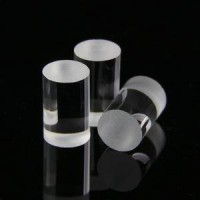
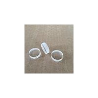
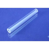
Product Name: Free-Standing GaN Substrates Brand: Finewin Application: Television Type: N-type Semiconductor Material: Compound Semiconductor Manufacturing Technology: Optoelectronic Semiconductor Materials: Gallium Nitride Substrates Thickness: 350um Size: 2inch to 4 Inch Trademark: FineWin Transport Package: Box Specification: 2INCH Origin: Jiaozuo City Henan Province Product Description Free-Standing GaN Substrates1. What is GaN substratesGallium Nitride is one kind of wide-gap compound semiconductors. It is made with original HVPE method and wafer processing technology, which has been originally developed for many years.2.ApplicationLaser diodes for Blu-ray Disc™players and light projectorsFuture application: GaN PN-diode with high breakdown voltage over 3,000V and low on-resistance of 1mΩ·cm2long-lived, efficient and reliable optoelectronic and electronic deviceshigh brightness LEDs for general lighting and high power, high frequency transistors for cellular phone base stations and defence applications.3.Product available2"GaN substratessmall pieces (10*10.5mm) for your testing usageGaN-template with highly doped n-type layer (n=<1e19/cm3)Ntype (undoped), Ntype (Ge doped), and Semi-insulating(Fe doped) substrates are availableNon-polar and semi-polar GaN substrates4. Featureshigh crystalline, good uniformity, and superior surface qualityXRD-FWHM002102350μm FSGaN25-4520-555. SpecificationItemGaN-FS-C-U-C50GaN-FS-C-N-C50GaN-FS-C-SI-C50DimensionsФ 50.8 mm ± 1 mmThickness350 ± 25 µmUseable Surface Area> 90%OrientationC-plane (0001) off angle toward M-Axis 0.35°± 0.15°Orientation Flat(1-100) ± 0.5°, 16.0 ± 1.0 mmSecondary Orientation Flat(11-20) ± 3°, 8.0 ± 1.0 mmTTV(Total Thickness Variation)≤ 15 µmBOW≤ 20 µmConduction TypeN-type(Undoped)N-type(Ge-doped)Semi-Insulating(Fe-doped)Resistivity(300K< 0.5 Ω·cm< 0.05 Ω·cm>106 Ω·cmDislocation Density1~9x105 cm-25x105 cm-2~3x106 cm-21~9x105 cm-21~3x106 cm-21~3x106 cm-2PolishingFront Surface: Ra < 0.2 nm. Epi-ready polishedBack Surface: Fine groundPackagePackaged in a class 100 clean room environment, in single wafer containers, under a nitrogen atmosphere.6. Pictures